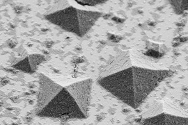
The process of crystallization, in which atoms or molecules line up in orderly arrays like soldiers in formation, is the basis for many of the materials that define modern life, including the silicon in microchips and solar cells. But while many useful applications for crystals involve their growth on solid surfaces (rather than in solution), there has been a dearth of good tools for studying this type of growth.
Now, a team of researchers at MIT and Draper has found a way to reproduce the growth of crystals on surfaces, but at a larger scale that makes the process much easier to study and analyze. The new approach is described in a paper in the journal Nature Materials, by Robert Macfarlane and Leonardo Zomberg at MIT, and Diana Lewis PhD ’19 and David Carter at Draper.
Rather than assembling these crystals from actual atoms, the key to making the process easy to observe and quantify was the use of “programmable atom equivalents,” or PAEs, Macfarlane explains. This works because the ways atoms line up into crystal lattices is entirely a matter of geometry and doesn’t rely on the specific chemical or electronic properties of its constituents.
The team used spherical nanoparticles of gold, coated with specially selected single strands of genetically engineered DNA, giving the particles roughly the appearance of Koosh balls. Single DNA strands have the inherent property of attaching themselves tightly to the corresponding reciprocal strands, to form the classic double helix, so this configuration provides a surefire way of getting the particles to align themselves in precisely the desired way.
“If I put a very dense brush of DNA on the particle, it’s going to make as many bonds with as many nearest neighbors as it can,” Macfarlane says. “And if you design everything appropriately and process it correctly, they will form ordered crystal structures.” While that process has been known for some years, this work is the first to apply that principle to study the growth of crystals on surfaces.
“Understanding how crystals grow upward from a surface is incredibly important for a lot of different fields,” he says. The semiconductor industry, for example, is based on the growth of large single-crystal or multi-crystalline materials that must be controlled with great precision, yet the details of the process are difficult to study. That’s why the use of oversized analogs such as the PAEs can be of such benefit.
The PAEs, he says, “crystallize in exactly the same pathways that molecules and atoms do. And so they are a very nice proxy system for understanding how crystallization occurs.” With this system, the properties of the DNA dictate how the particles assemble and the 3D configuration they end up in.
They designed the system such that the crystals nucleate and grow starting from a surface and “by tailoring the interactions both between particles, and between the particles and the DNA-coated surface, we can dictate the size, the shape, the orientation and the degree of anisotropy (directionality) in the crystal,” Macfarlane says.
“By understanding the process this is going through to actually form these crystals, we can potentially use that to understand crystallization processes in general,” he adds.
He explains that not only are the resulting crystal structures about 100 times larger than the actual atomic ones, but their formation processes are also much slower. The combination makes the process much easier to analyze in detail. Earlier methods of characterizing such crystalline structures only showed their final states, thus missing complexities in the formation process.
“I could change the DNA sequence. I can change the number of DNA strands in the particle. I can change the size of the particle and I can tweak each of these individual handles independently,” Macfarlane says. “So if I wanted to be able to say, OK, I hypothesize that this particular structure might be favored under these conditions if I tuned the energetics in such a way, that’s a much easier system to study with the PAEs than it would be with atoms themselves.”
The system is very effective, he says, but DNA strands modified in a manner that allows for attachment to nanoparticles can be quite expensive. As a next step, the Macfarlane lab has also developed polymer-based building blocks that show promise in replicating these same crystallization processes and materials, but can be made inexpensively at a multigram scale.
The work was funded by the Air Force Office of Scientific Research and supported by a Draper fellowship and the National Science Foundation and used facilities of the Materials Technology Laboratory at MIT.


