A broad class of materials called perovskites is considered one of the most promising avenues for developing new, more efficient solar cells. But the virtually limitless number of possible combinations of these materials’ constituent elements makes the search for promising new perovskites slow and painstaking.
Now, a team of researchers at MIT and several other institutions has accelerated the process of screening new formulations, achieving a roughly ten-fold improvement in the speed of the synthesis and analysis of new compounds. In the process, they have already discovered two sets of promising new perovskite-inspired materials that are worthy of further study.
Their findings are described this week in the journal Joule, in a paper by MIT research scientist Shijing Sun, professor of mechanical engineering Tonio Buonassisi, and 16 others at MIT, in Singapore, and at the National Institute of Standards and Technology in Maryland.
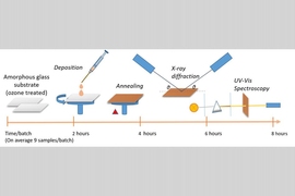
Somewhat surprisingly, although partial automation was employed, most of the improvements in throughput speed resulted from workflow ergonomics, says Buonassisi. That involves more traditional systems efficiencies, often derived by tracking and timing the many steps involved: synthesizing new compounds, depositing them on a substrate to crystallize, and then observing and classifying the resulting crystal formations using multiple techniques.
“There’s a need for accelerated development of new materials,” says Buonassisi, as the world continues to move toward solar energy, including in regions with limited space for solar panels. But the typical system for developing new energy-conversion materials can take 20 years, with significant upfront capital costs, he says. His team’s aim is to cut that development time to under two years.
Essentially, the researchers developed a system that allows a wide variety of materials to be made and tested in parallel. “We’re now able to access a large range of different compositions, using the same materials synthesis platform. It allows us to explore a vast range of parameter space,” he says.
Perovskite compounds consist of three separate constituents, traditionally labeled as A, B, and X site ions, each of which can be any one of a list of candidate elements, forming a very large structural family with diverse physical properties. In the field of perovskite and perovskite-inspired materials for photovoltaic applications, the B-site ion is typically lead, but a major effort in perovskite research is to find viable lead-free versions that can match or exceed the performance of the lead-based varieties.
While more than a thousand potentially useful perovskite formulations have been predicted theoretically, out of millions of theoretically possible combinations, only a small fraction of those has been produced experimentally so far, highlighting the need for an accelerated process, the researchers say.
For the experiments, the team selected a variety of different compositions, each of which they mixed in a solution and then deposited on a substrate, where the material crystallized into a thin film. The film was then examined using a technique called X-ray diffraction, which can reveal details of how the atoms are arranged in the crystal structure. These X-ray diffraction patterns were then initially classified with the help of a convolutional neural network system to speed up that part of the process. That classification step alone, Buonassisi says, initially took three to five hours, but by applying machine learning, this was slashed to 5.5 minutes while maintaining 90 percent accuracy.
Already, in their initial testing of the system, the team explored 75 different formulations in about a tenth of the time it previously would have taken to synthesize and characterize that many. Among those 75, they found two new lead-free perovskite systems that exhibit promising properties that might have potential for high-efficiency solar cells.
In the process, they produced four compounds in thin-film form for the first time; thin films are the desirable form for use in solar cells. They also found examples of “nonlinear bandgap tunability” in some of the materials, an unexpected characteristic that relates to the energy level needed to excite an electron in the material, which they say opens up new pathways for potential solar cells.
The team says that with further automation of parts of the process, it should be possible to continue to increase the processing speed, making it anywhere from 10 to 100 times as fast. Ultimately, Buonassisi says, it’s all about getting solar power to be as inexpensive as possible, continuing the technology’s already remarkable plunge. The aim is to bring economically sustainable prices below 2 cents per kilowatt-hour, he says, and getting there could be the result of a single breakthrough in materials: “All you have to do is make one material” that has just the right combination of properties — including ease of manufacture, low cost of materials, and high efficiency at converting sunlight.
“We’re putting all the experimental pieces in place so we can explore faster,” he says.
The work was supported by Total SA through the MIT Energy Initiative, by the National Science Foundation, and Singapore’s National Research Foundation through the Singapore-MIT Alliance for Research and Technology.


