Sometimes things that are technically defects, such as imperfections in a material’s crystal lattice, can actually produce changes in properties that open up new kinds of useful applications. New research from a team at MIT shows that such imperfections in a family of materials known as insulating metal oxides may be key to their performance for a variety of high-tech applications, such as nonvolatile memory chips and energy conversion technologies.
The findings are reported this week in the journal Physical Review Letters, in a paper by MIT Associate Professor Bilge Yildiz, Professor and Associate Provost Krystyn Van Vliet, and former postdoc Mostafa Youssef.
These metal oxide materials have been investigated by many researchers, Yildiz says, and “their properties are highly governed by the number and the kind of defects that are present.” When subjected to strong driving forces, such as strong electric fields, “the behavior of such defects had not been well-understood,” she says.
Researchers do have a well-established theoretical understanding of how perfectly structured versions of these insulating metal oxides function under a variety of conditions, such as in strong electric fields, but there was no such theory to describe the materials when they contain common types of defects, according to Yildiz. Understanding these effects quantitatively is important in order to develop this promising family of materials for potential applications including new types of low-energy computer memory and processing devices, electrically based refrigeration, and electro-catalytic energy-conversion devices such as fuel cells.
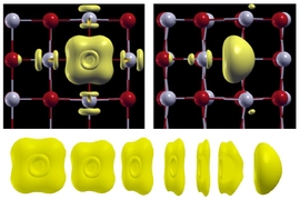
The team demonstrated a theoretical framework and showed how the stability and structure of a point defect is altered under strong electric fields. They took a common defect called a neutral oxygen vacancy — a place where an oxygen atom should appear in the lattice but instead two electrons are trapped. Their results have quantified the polarization behavior of the material with this defect, in an electric field.
“The oxygen vacancies in particular are very important in electronic and electrochemical applications,” says Yildiz, who holds joint appointments in the departments of Nuclear Science and Engineering and Materials Science and Engineering.
In many of these applications, she says, there can be an internal voltage gradient created within the thin-film material, and this “electric potential” gradient causes strong electric fields. Understanding the effects of those fields is essential for the design of certain new devices.
“Most of the work in this area is experimental,” Yildiz says. “You take a thin film, you put it in an electric field, and you do measurements.” But in such experiments, the effects of the local electric potential and the electric field are convoluted, making it very hard to understand the results. “It’s impossible to resolve them from each other, so you need to have a theory” to account for the effects, she adds.
The researchers have now devised a new theoretical framework that allows them to isolate the electric field effect from the electric potential effect, and quantify both independently. This allowed them to make very specific predictions that are different from those produced by classical theory and should make it possible to validate the new model experimentally within a year, Yildiz says.
The findings should help enable the development of some important potential applications, she says. One is in a new type of computer memory device known as resistive switching memory, which provides fast switching speeds using very little energy. These memory devices rely on the presence of defects.
“The way they switch their resistance state [to record data] depends on the defect type, content, and distribution,” she says. “In order to model the device behavior, you should be able to model how the applied strong electric fields alter the defect structure, concentration, and distribution.” That’s what this new work enables: “If you know quantitatively the effects of both the potential and the field, then you can design your operating conditions to benefit from these effects.”
Understanding these effects is also important for other applications such as splitting water molecules to produce hydrogen at solid-liquid interfaces, electronic devices that rely on oxide-oxide interfaces, or other electrochemical processes using these materials as catalysts, where defects serve as the sites that enable the interactions.
The materials the team studied belong to a class known as alkaline-earth-metal binary oxides, whose constituents are “among the most abundant class of materials on Earth,” Yildiz says. “[This class is] cheap, abundant, and has tunable properties,” making it promising for many applications. But she adds that the theoretical approach they took will now be applied much more broadly, to many other kinds of oxide materials and to other kinds of defects within them besides the neutral oxygen vacancies.
“This work establishes a new paradigm for the study of defects in semiconductors, by setting up the necessary mathematics for the calculation of the defect formation energy in electrically stimulated defective crystals,” says Cesare Franchini, an associate professor of computational materials physics at the University of Vienna, who was not involved in this work. “This work extends the current theories which connect thermodynamics with electric polarization, and will be beneficial for virtually all applications in which defects (and their tunability by electric stimuli) are an asset, including catalysis, electronics, and electrocaloric devices.”
The research was supported by the MRSEC Program of the National Science Foundation and used resources of the National Energy Research Scientific Computing Center, a Department of Energy Office of Science User Facility supported by the Office of Science of the U.S. Department of Energy.


