Skip to content ↓

Silicon can be made to melt in reverse

Material that shows melting while cooling might someday lead to applications in solar cells and other devices
Press Inquiries

Press Contact:

Jen Hirsch
Phone: 617-253-2700
MIT News Office

Media Download

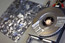
A tiny silicon chip — the glowing orange square at the center of this special heating device — is heated to a temperature well below silicon’s melting point, and then very slowly cooled down. The chip inside this heating device was placed in the path of a synchrotron beam to probe its changes at a molecular level as it went through the retrograde melting process.
Download Image
Caption: A tiny silicon chip — the glowing orange square at the center of this special heating device — is heated to a temperature well below silicon’s melting point, and then very slowly cooled down. The chip inside this heating device was placed in the path of a synchrotron beam to probe its changes at a molecular level as it went through the retrograde melting process.
Credits: Photo: Patrick Gillooly
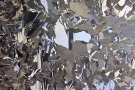
A wafer of silicon, which is the most widely used material for computer chips and solar cells.
Download Image
Caption: A wafer of silicon, which is the most widely used material for computer chips and solar cells.
Credits: Photo: Patrick Gillooly
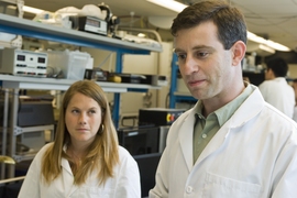
Postdoctoral fellow Bonna Newman PhD ’08 and Tonio Buonassisi, the SMA Assistant Professor of Mechanical Engineering and Manufacturing, discuss their work studying the retrograde melting property of silicon.
Download Image
Caption: Postdoctoral fellow Bonna Newman PhD ’08 and Tonio Buonassisi, the SMA Assistant Professor of Mechanical Engineering and Manufacturing, discuss their work studying the retrograde melting property of silicon.
Credits: Photo: Patrick Gillooly

*Terms of Use:

Images for download on the MIT News office website are made available to non-commercial entities, press and the general public under a Creative Commons Attribution Non-Commercial No Derivatives license. You may not alter the images provided, other than to crop them to size. A credit line must be used when reproducing images; if one is not provided below, credit the images to "MIT."

Close
A tiny silicon chip — the glowing orange square at the center of this special heating device — is heated to a temperature well below silicon’s melting point, and then very slowly cooled down. The chip inside this heating device was placed in the path of a synchrotron beam to probe its changes at a molecular level as it went through the retrograde melting process.
Caption:
A tiny silicon chip — the glowing orange square at the center of this special heating device — is heated to a temperature well below silicon’s melting point, and then very slowly cooled down. The chip inside this heating device was placed in the path of a synchrotron beam to probe its changes at a molecular level as it went through the retrograde melting process.
Credits:
Photo: Patrick Gillooly
A wafer of silicon, which is the most widely used material for computer chips and solar cells.
Caption:
A wafer of silicon, which is the most widely used material for computer chips and solar cells.
Credits:
Photo: Patrick Gillooly
Postdoctoral fellow Bonna Newman PhD ’08 and Tonio Buonassisi, the SMA Assistant Professor of Mechanical Engineering and Manufacturing, discuss their work studying the retrograde melting property of silicon.
Caption:
Postdoctoral fellow Bonna Newman PhD ’08 and Tonio Buonassisi, the SMA Assistant Professor of Mechanical Engineering and Manufacturing, discuss their work studying the retrograde melting property of silicon.
Credits:
Photo: Patrick Gillooly

Like an ice cube on a warm day, most materials melt — that is, change from a solid to a liquid state — as they get warmer. But a few oddball materials do the reverse: They melt as they get cooler. Now a team of researchers at MIT has found that silicon, the most widely used material for computer chips and solar cells, can exhibit this strange property of “retrograde melting” when it contains high concentrations of certain metals dissolved in it.

The material, a compound of silicon, copper, nickel and iron, “melts” (actually turning from a solid to a slush-like mix of solid and liquid material) as it cools below 900 degrees Celsius, whereas silicon ordinarily melts at 1414 degrees C. The much lower temperatures make it possible to observe the behavior of the material during melting, based on specialized X-ray fluorescence microprobe technology using a synchrotron — a type of particle accelerator — as a source.

The material and its properties are described in a paper just published online in the journal Advanced Materials. Team leader Tonio Buonassisi, the SMA Assistant Professor of Mechanical Engineering and Manufacturing, is the senior author, and the lead authors are Steve Hudelson MS ’09, and postdoctoral fellow Bonna Newman PhD ’08.

The findings could be useful in lowering the cost of manufacturing some silicon-based devices, especially those in which tiny amounts of impurities can significantly reduce performance. In the material that Buonassisi and his researchers studied, impurities tend to migrate to the liquid portion, leaving regions of purer silicon behind. This could make it possible to produce some silicon-based devices, such as solar cells, using a less pure, and therefore less expensive, grade of silicon that would be purified during the manufacturing process.

“If you can create little liquid droplets inside a block of silicon, they serve like little vacuum cleaners to suck up impurities,” Buonassisi says. This research could also lead to new methods for making arrays of silicon nanowires — tiny tubes that are highly conductive to heat and electricity.

Buonassisi predicted in a 2007 paper that it should be possible to induce retrograde melting in silicon, but the conditions needed to produce such a state, and to study it at a microscopic level, are highly specialized and have only recently become available. To create the right conditions, Buonassisi and his team had to adapt a microscope “hot-stage” device that allowed the researchers to precisely control the rate of heating and cooling. And to actually observe what was happening as the material was heated and cooled, they drew upon high-power synchrotron-based X-ray sources at Lawrence Berkeley National Laboratory in California and at Argonne National Laboratory in Illinois (researchers from both national labs are co-authors of the paper).

The research was supported by the U.S. Department of Energy, the National Science Foundation, the Clare Booth Luce Foundation, Doug Spreng and the Chesonis Family Foundation, and some equipment was provided by McCrone Microscopes & Accessories.

The material for the tests consisted of a kind of sandwich made from two thin layers of silicon, with a filling of copper, nickel and iron between them. This was first heated enough to cause the metals to dissolve into the silicon, but below silicon’s melting point. The amount of metal was such that the silicon became supersaturated — that is, more of the metal was dissolved in the silicon than would normally be possible under stable conditions. For example, when a liquid is heated, it can dissolve more of another material, but then when cooled down it can become supersaturated, until the excess material precipitates out.

In this case, where the metals were dissolved into the solid silicon, “if you begin cooling it down, you hit a point where you induce precipitation, and it has no choice but to precipitate out in a liquid phase,” Buonassisi says. It is at that point that the material melts.

Matthias Heuer, a senior research scientist at Calisolar, a solar-energy startup company, says this work is “unique and new to our field,” and it “allows some very good insight into how transition metals and structural defects interact.” But he adds that there are a number of questions still to be answered in follow-up research: “Now that we know liquid inclusions can form, the question is, how efficient as sinks for impurities are they? How stable are they? Can they keep the impurities localized during other process steps — for example, during the final firing process of a solar cell?”
Related Links

Related Topics

More MIT News

Gene Keselman headshot

Faces of MIT: Gene Keselman

At MIT, Keselman is a lecturer, executive director, managing director, and innovator. Additionally, he is a colonel in the Air Force Reserves, board director, and startup leader.

Read full story